Fermi Level In Semiconductors : Fermi-Energy Level for Extrinsic Semiconductor - Physics ... : Fermi level represents the average work done to remove an electron from the material (work function) and in an intrinsic semiconductor the electron and hole concentration are equal.
Fermi Level In Semiconductors : Fermi-Energy Level for Extrinsic Semiconductor - Physics ... : Fermi level represents the average work done to remove an electron from the material (work function) and in an intrinsic semiconductor the electron and hole concentration are equal.. Is fermi level definition different from what is know as usual? * for an given semiconductor at a constant temperature, the value of ni is constant, and independent of the fermi energy. Thus with an increase in the temperature of an extrinsic semiconductor. We look at some formulae whixh will help us to solve sums. The electrical conductivity of the semiconductor depends upon the total no of electrons moved to the conduction band from the valence band.
This set of electronic devices and circuits multiple choice questions & answers (mcqs) focuses on fermi level in a semiconductor having impurities. Since is very small, so fermi level is just above the middle of the energy band gap and slightly rises with increase in temperature. In semiconductors the position of the. What does it mean that the fermi level for some semiconductors lie in the band gap? Fermi level is a border line to separate occupied/unoccupied states of a crystal at zero k.
Semiconductors/PN Junctions - Wikibooks, open books for an ... from upload.wikimedia.org It can be written as. Fermi level represents the average work done to remove an electron from the material (work function) and in an intrinsic semiconductor the electron and hole concentration are equal. 10 we can deduce that the fermi level ef must be in the middle of the bandgap for an intrinsic semiconductor, as seen in figure 4. In all cases, the position was essentially independent of the metal. Is fermi level definition different from what is know as usual? The fermi level is on the order of electron volts (e.g., 7 ev for copper), whereas the thermal energy kt is only about 0.026 ev at 300k. Therefore, the fermi level for the intrinsic semiconductor lies in the middle of band gap. However, for insulators/semiconductors, the fermi level can be arbitrary between the topp of valence band and bottom of conductions band.
What does it mean that the fermi level for some semiconductors lie in the band gap?
Each pentavalent impurity donates a free electron. Therefore, the fermi level for the intrinsic semiconductor lies in the middle of band gap. We mentioned earlier that the fermi level lies within the forbidden gap, which basically results from the need to maintain equal concentrations of electrons and (15) and (16) be equal at all temperatures, which yields the following expression for the position of the fermi level in an intrinsic semiconductor The occupancy of semiconductor energy levels. Now what does it mean when the fermi level lies in the band gap or instead in one of the bands? • the fermi function and the fermi level. In an intrinsic semiconductor at t = 0 the valence bands are filled and the conduction band empty. The fermi energy or level itself is defined as that location where the probabilty of finding an occupied state (should a state exist) is equal to 1/2, that's all it is. Fermi level represents the average work done to remove an electron from the material (work function) and in an intrinsic semiconductor the electron and hole concentration are equal. 5 fermi level and variation of fermi level with temperature in an intrinsic semiconductor. Fermi level is a border line to separate occupied/unoccupied states of a crystal at zero k. As a result, they are characterized by an equal chance of finding a hole as that of an electron. It is shown that the position of the stabilization energy with respect to the band edges determines the maximum free carrier.
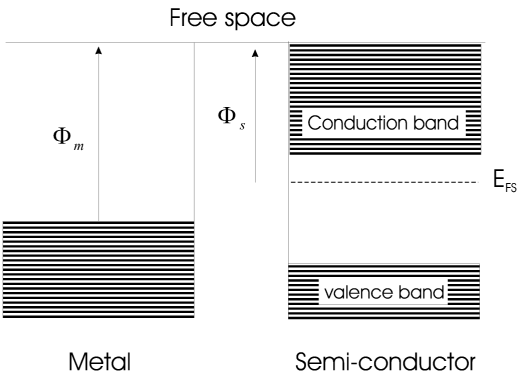
Fermi level (ef) and vacuum level (evac) positions, work function (wf), energy gap (eg), ionization energy (ie), and electron affinity (ea) are parameters of great importance for any electronic material, be it a metal, semiconductor, insulator, organic, inorganic or hybrid. Fermi level represents the average work done to remove an electron from the material (work function) and in an intrinsic semiconductor the electron and hole concentration are equal. Chapter 5 semiconductor in equilibrium. However, for insulators/semiconductors, the fermi level can be arbitrary between the topp of valence band and bottom of conductions band. Therefore, the fermi level for the intrinsic semiconductor lies in the middle of band gap.
Chapter2.2.3;2.2.4;2.2.5;Insulator,Semi-conductor,Metal ... from archive.cnx.org What does it mean that the fermi level for some semiconductors lie in the band gap? The fermi level does not include the work required to remove the electron from wherever it came from. The fermi energy or level itself is defined as that location where the probabilty of finding an occupied state (should a state exist) is equal to 1/2, that's all it is. Fermi level in an intrinsic semiconductor. Dopant atoms and energy levels. It is shown that the position of the stabilization energy with respect to the band edges determines the maximum free carrier. Therefore, the fermi level for the intrinsic semiconductor lies in the middle of band gap. In all cases, the position was essentially independent of the metal.
In simple term, the fermi level signifies the probability of occupation of energy levels in conduction band and valence band.
It is well estblished for metallic systems. Dopant atoms and energy levels. It is shown that the position of the stabilization energy with respect to the band edges determines the maximum free carrier. It can be written as. Charge carrier densities and fermi level in extrinsic semiconductors strongly depend on temperature and impurity density. Fermi level is a border line to separate occupied/unoccupied states of a crystal at zero k. Uniform electric field on uniform sample 2. Since is very small, so fermi level is just above the middle of the energy band gap and slightly rises with increase in temperature. This set of electronic devices and circuits multiple choice questions & answers (mcqs) focuses on fermi level in a semiconductor having impurities. Fermi level in the middle of forbidden band indicates equal concentration of free electrons and holes. Then the fermi level approaches the middle of forbidden energy gap. Increases the fermi level should increase, is that. It is a thermodynamic quantity usually denoted by µ or ef for brevity.
P = n = ni. • the fermi function and the fermi level. In fact, this level is. Thus with an increase in the temperature of an extrinsic semiconductor. Increases the fermi level should increase, is that.
Fermi Level In Intrinsic Semiconductor - Solved Model 2 ... from qph.fs.quoracdn.net Intrinsic semiconductors are the pure semiconductors which have no impurities in them. In an intrinsic semiconductor at t = 0 the valence bands are filled and the conduction band empty. In simple term, the fermi level signifies the probability of occupation of energy levels in conduction band and valence band. 10 we can deduce that the fermi level ef must be in the middle of the bandgap for an intrinsic semiconductor, as seen in figure 4. Now what does it mean when the fermi level lies in the band gap or instead in one of the bands? Fermi level in the middle of forbidden band indicates equal concentration of free electrons and holes. Here's an overview using a nice diagram from wikipedia The occupancy of semiconductor energy levels.
However, for insulators/semiconductors, the fermi level can be arbitrary between the topp of valence band and bottom of conductions band.
Fermi level in the middle of forbidden band indicates equal concentration of free electrons and holes. Chapter 5 semiconductor in equilibrium. The fermi level is on the order of electron volts (e.g., 7 ev for copper), whereas the thermal energy kt is only about 0.026 ev at 300k. The occupancy of semiconductor energy levels. Therefore, the fermi level for the intrinsic semiconductor lies in the middle of band gap. * for an given semiconductor at a constant temperature, the value of ni is constant, and independent of the fermi energy. What does it mean that the fermi level for some semiconductors lie in the band gap? Fermi level in extrinsic semiconductors. We mentioned earlier that the fermi level lies within the forbidden gap, which basically results from the need to maintain equal concentrations of electrons and (15) and (16) be equal at all temperatures, which yields the following expression for the position of the fermi level in an intrinsic semiconductor Fermi level is a border line to separate occupied/unoccupied states of a crystal at zero k. In semiconductors the position of the. Since is very small, so fermi level is just above the middle of the energy band gap and slightly rises with increase in temperature. It is shown that the position of the stabilization energy with respect to the band edges determines the maximum free carrier.


0 Komentar